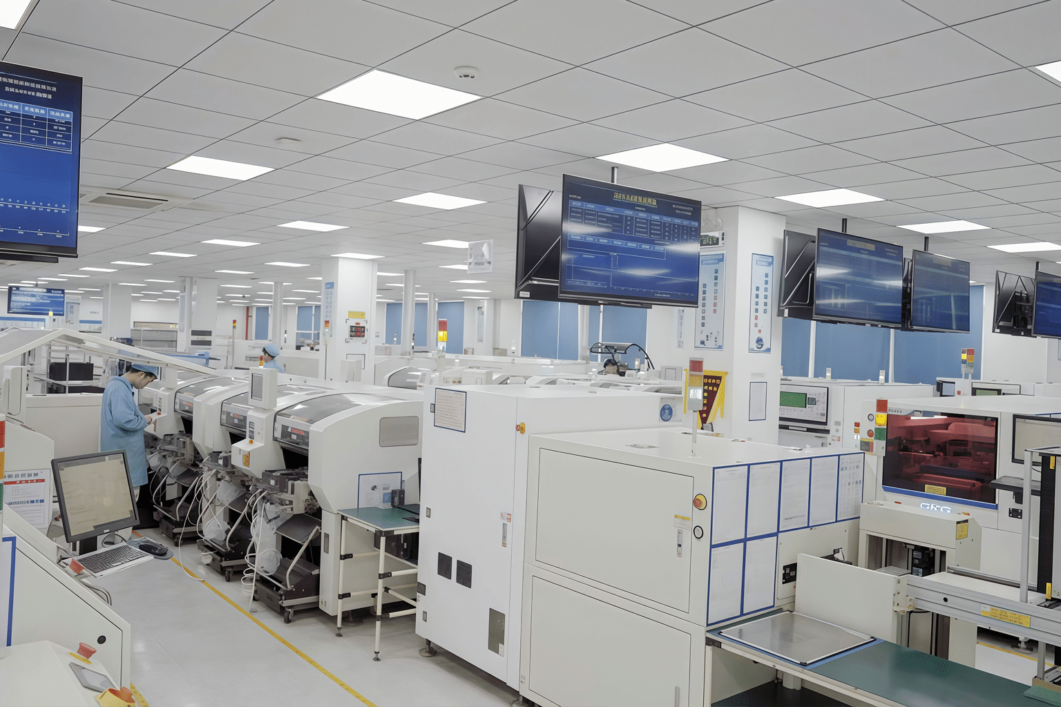
AOI vs SPI on the SMT Line
One checks the paste, the other checks the part. Use both at the right stage.
Read More →KOMKIA Insights
Practical notes on PCB fabrication, PCBA assembly, component strategy and manufacturing economics — written by the KOMKIA engineering team.
Latest Articles
One checks the paste, the other checks the part. Use both at the right stage.
Read More →
A trace is a resistor you did not draw. Size it before it heats.
Read More →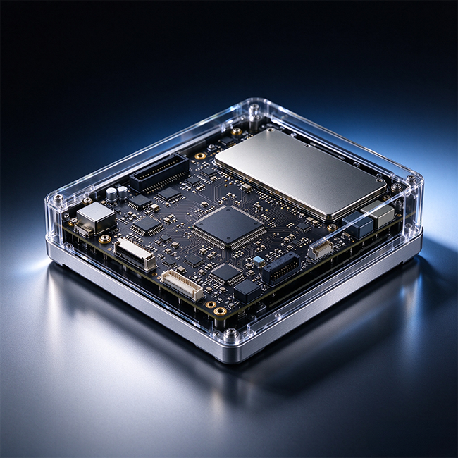
Unwanted radiation is a design choice you made by omission. Close the loops.
Read More →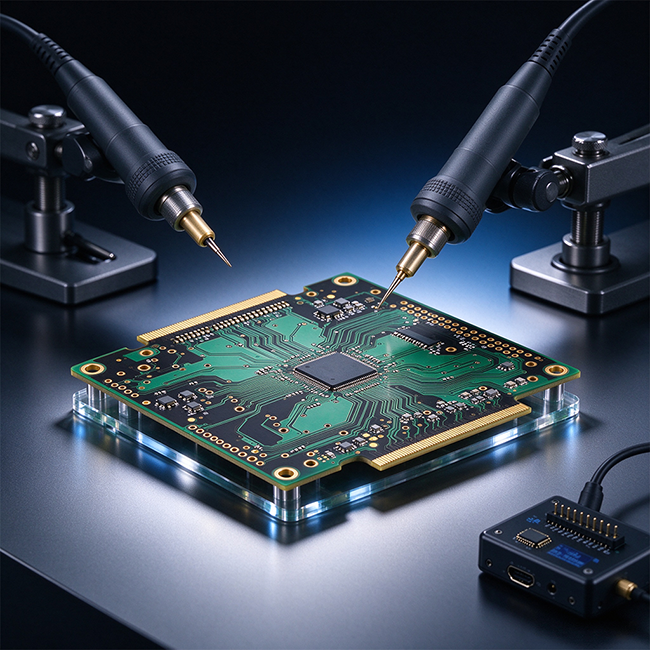
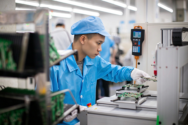
Vias that do not go all the way buy routing space at process cost.
Read More →
Copper in the holes is what makes a via a via. Plating quality is board quality.
Read More →
Moisture inside a package turns reflow into a small explosion. Know your level.
Read More →
When the board or parts cannot take 260 °C, drop the peak with a low-temp alloy.
Read More →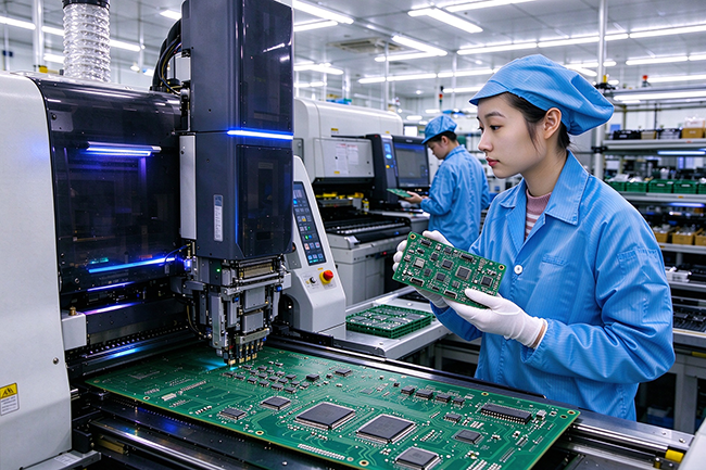
Without fiducials, the machine is guessing. A few marks fix the whole panel.
Read More →