The PCB Plating Process
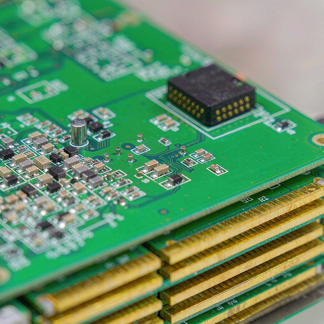
Electroless seed, electrolytic build and balance against etch-back decide barrel and surface uniformity.
Seed layer
Electroless copper makes the hole conductive before plating.
Barrel fill
Uniform throw into deep holes separates good shops.
Thickness control
Spec minimum barrel and surface per IPC class.
Key Takeaways
Key Takeaways
- Seed before electrolytic plating.
- Uniform deep-hole throw matters most.
- Spec barrel thickness per IPC.