Overview
Capabilities & Process
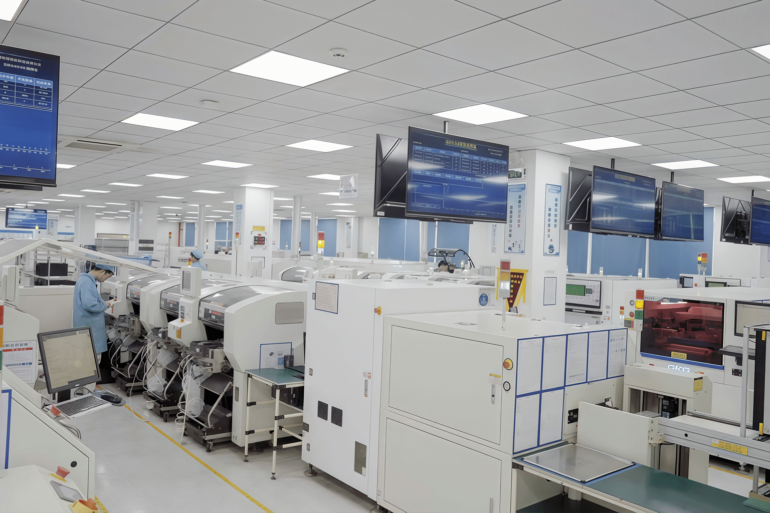
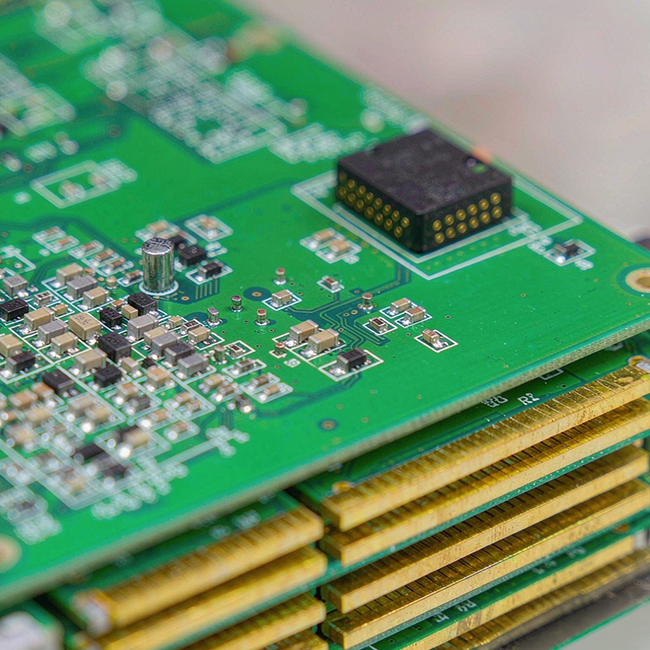
KOMKIA provides a complete, vertically integrated electronics manufacturing chain — from bare board fabrication to final box build — under one roof with consistent quality systems.
Explore our full capability table and the end-to-end production process that takes your design from file to finished product.
Process Steps
End-to-End Process
1 · Engineering Review
DFM/DFA and quote within hours.
2 · PCB Fabrication
Inner-layer to final routing and finish.
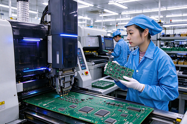
3 · SMT & THT
High-speed placement and wave/selective solder.
4 · Inspection
SPI, AOI and X-ray for BGAs.
5 · Test
ICT, FCT and burn-in as required.
6 · Box Build & Ship
Integration, packaging and logistics.
Specs
Combined Capabilities
| Parameter | Capability |
|---|---|
| PCB Layers | 1 – 32 layers |
| SMT Lines | 16 lines |
| Quality Grade | IPC Class 3 |
| Order Quantity | 1 pc – 10M+ pcs |
| Certifications | ISO 9001, ISO 13485, IATF 16949, RoHS, UL |
| Testing | AOI, X-ray, ICT, FCT, burn-in |
| Turnkey | Fab + Assembly + Box Build |
| Lead Time | Prototype 24h, volume 1–2 weeks |
Gallery
Factory & Process