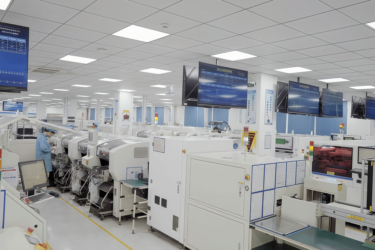
Tin Whisker Risks and Mitigation
Pure tin can grow microscopic hairs that short your circuit. Mitigate by design.
Read More →KOMKIA Insights
Practical notes on PCB fabrication, PCBA assembly, component strategy and manufacturing economics — written by the KOMKIA engineering team.
Latest Articles
Pure tin can grow microscopic hairs that short your circuit. Mitigate by design.
Read More →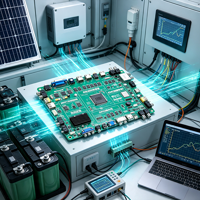
The finish is your pad interface. Pick it for solderability, planarity and cost.
Read More →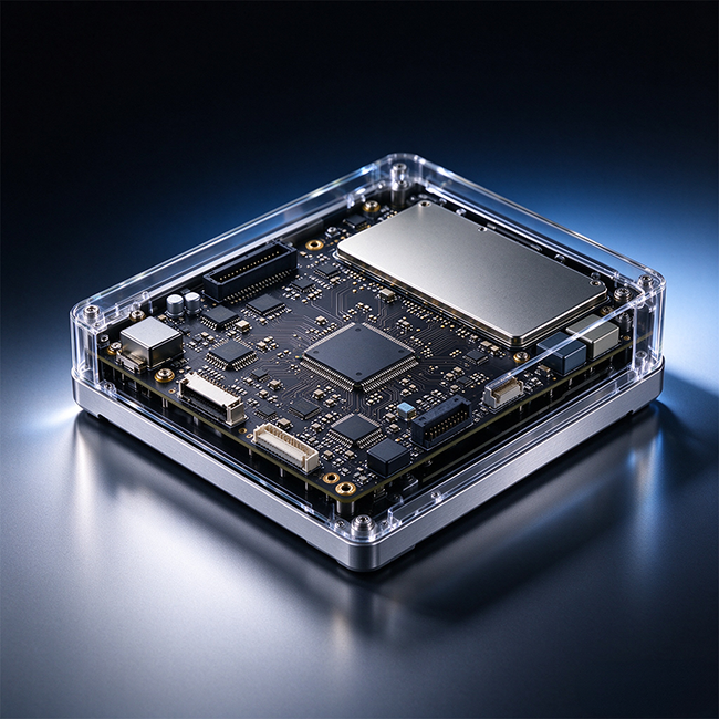
Run it hot now so it does not fail later. Burn-in flushes early-life defects.
Read More →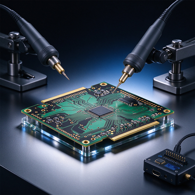
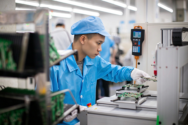
Plated board edges and half-holes let boards plug into boards.
Read More →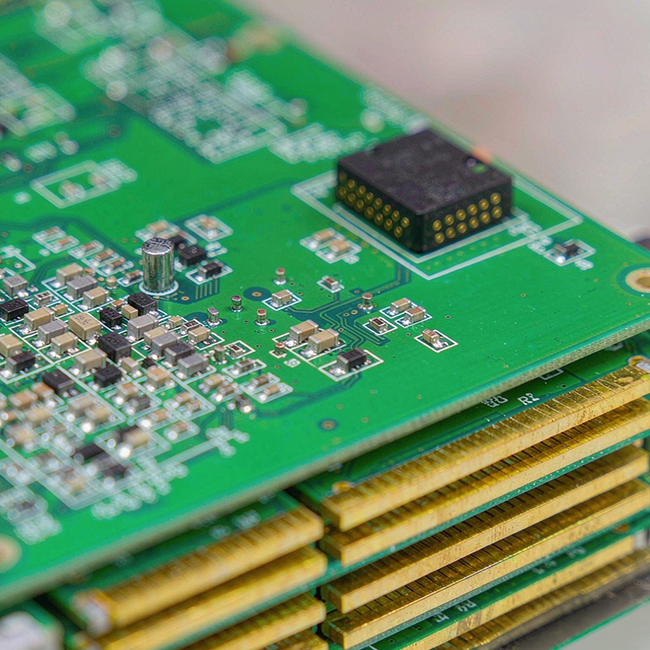
In-Circuit Test probes every node while the board is powered down.
Read More →
Layer count is the biggest single cost driver. Design it down.
Read More →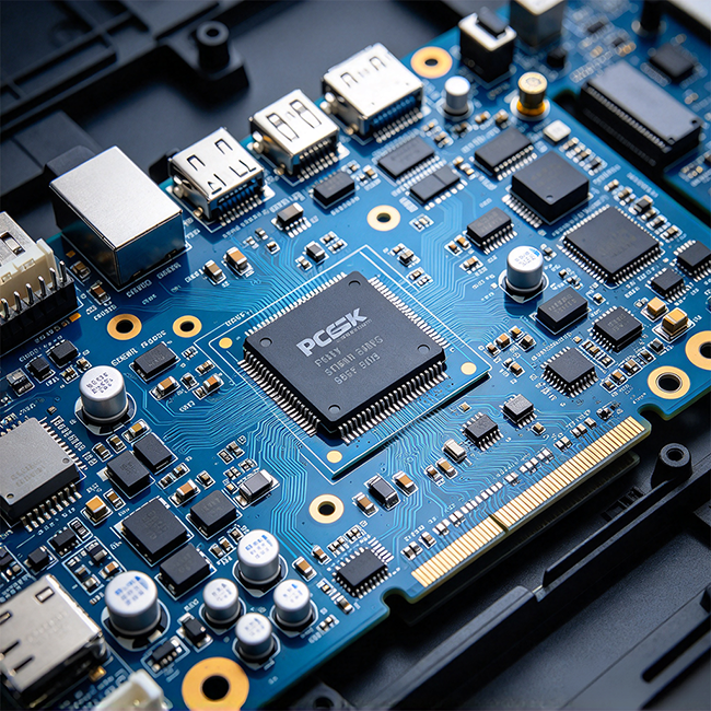
Restricted substances are a market-access gate, not a suggestion.
Read More →
Box build is where the board meets the world. Harness quality decides the last mile.
Read More →