Overview
PCB & PCBA Design
Good design is the cheapest quality you can buy. KOMKIA's engineering team supports schematic capture, PCB layout and design-for-manufacture reviews so your product is optimized before it reaches the line.
From concept to optimized Gerber and BOM, we help you reduce risk, cost and time-to-market.
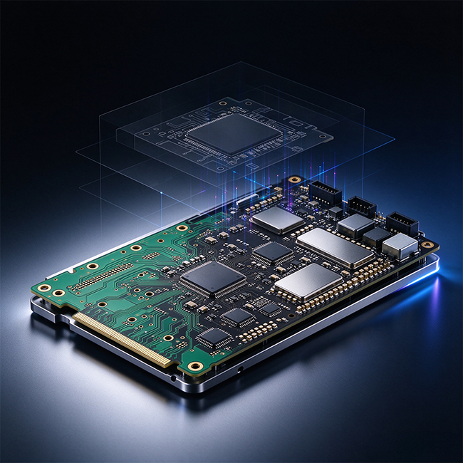
Engineering
Design Services
Schematic Design
Capture and review of your circuit schematic.
PCB Layout
High-speed, RF and dense multilayer layout.
DFM / DFA Review
Free Valor checks to ensure manufacturability.
Signal Integrity
Impedance and SI/PI analysis for high-speed.
BOM Creation
Sourcing-friendly, cost-optimized BOM.
Value
Design Value
Faster Time-to-Market
Optimized designs avoid costly respins.
Lower Cost
Value-engineered BOM and processes.
Higher Yield
Manufacturable layouts from day one.
Specs
Design Capabilities
| Parameter | Capability |
|---|---|
| Disciplines | Analog, Digital, Mixed-signal, RF, Power |
| Layers | Up to 32 layers |
| Tools | Altium, KiCad, Cadence, Mentor |
| Review | DFM, DFA, DFT, SI/PI |
| Deliverables | Gerber, ODB++, BOM, assembly drawing |
| Patents | 20+ invention & design patents |
Gallery
Design & Layout