EMI Shielding in PCB Design
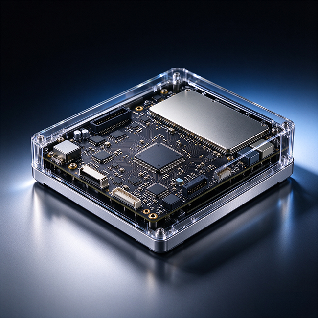
Stack-up, partitioning and filtering decide whether your board passes emissions. Good shielding starts on the laminate, not the can.
Stack-up first
A solid reference plane is the cheapest shield you have.
Partition
Keep noisy and sensitive circuits apart and guard the boundary.
Filter at the edge
Filter signals crossing partitions to stop accidental antennas.
Key Takeaways
Key Takeaways
- Reference planes are your first shield.
- Partition noisy from sensitive zones.
- Filter at every partition crossing.